
Exploring Chern Junctions: PbI2 Joins the Moiré Material Library
Chern junctions in Moir\'e-Patterned Graphene/PbI2
The paper introduces a novel Moiré heterostructure based on BN/graphene/PbI2, achieving a state-of-the-art ballistic transport regime at the charge neutrality point under high magnetic fields. Using magnetotransport, the authors identify "Chern junctions" and robust fractional conductance plateaus at 2/3 e^2/h, driven by Moiré-modulated topological states.
TL;DR
Researchers have successfully integrated PbI2—a semiconductor with heavy atoms and massive spin-orbit coupling (SOC)—into the Moiré superlattice family. By stacking it with graphene and hexagonal boron nitride (hBN), they discovered a new regime where longitudinal resistance completely vanishes at the charge neutrality point under high magnetic fields. The study reports the emergence of Chern junctions, which allow for ballistic transport and fractional conductance plateaus () through the internal "engineering" of topological domains.
The Motivation: Beyond Simple Moiré
The field of Moiré electronics has been dominated by twisted bilayer graphene and graphene/hBN. While these systems show incredible correlated physics (like superconductivity), they often lack the "heavy" ingredient: Spin-Orbit Coupling (SOC).
To realize more exotic states, like the elusive Kane-Mele topological insulator in a monolayer, researchers need to "inject" SOC into graphene without destroying its high mobility. PbI2 is an ideal candidate due to its large lattice constant (~2x graphene) and its role as a precursor in high-performance perovskites.
Methodology: Building the Super-Moiré
The team fabricated an hBN/graphene/PbI2 stack using dry-transfer techniques. The key was the alignment:
- Graphene/hBN twist: ~8°
- Graphene/PbI2 twist: ~31°
This specific configuration creates a large Moiré wavelength of approximately 16.4 nm. The heavy lead (Pb) atoms provide a proximity-induced SOC of roughly 12 meV, which is significantly higher than what is found in pristine graphene.
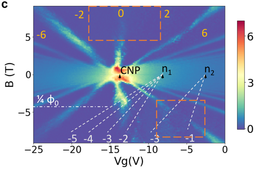 Figure 1: (c) The Landau fan diagram showing the vanishing Rxx (orange box) at the charge neutrality point.
Core Findings: The Chern Junction
The most striking result is the observation of a 2/3 fractional conductance plateau. In traditional physics, this usually requires complex p-n junctions created by external metal gates. Here, it happens intrinsically.
The authors suggest that the Moiré potential is so strong that it creates domains with different "flavors." When a region with a Moiré Chern number () meets a region with a conventional quantum Hall Chern number (), they form a Chern Junction. This junction acts as a "beam splitter" for electrons, leading to the quantized value.
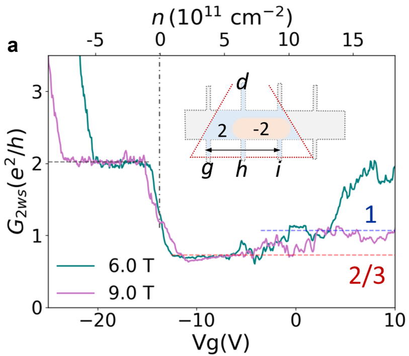 Figure 2: Conductance measurements showing the robust 2/3 plateau and the transition between different topological states.
Coherent Interference
Because these domain walls are extremely clean, the electrons don't just scatter randomly; they interfere. The team observed magnetoresistance fluctuations that were perfectly correlated across different parts of the device (separated by microns!). This is a smoking gun for quantum interference along Moiré domain boundaries.
Critical Analysis: A High-Field Topological Insulator?
The authors propose that the combination of the Hofstadter spectrum (the "fractal" energy levels of a Moiré lattice in a magnetic field) and the SOC from PbI2 drives the system into a high-magnetic-field topological insulator phase.
Strengths:
- High Mobility: Unlike many TMD-based structures, this device maintains a mobility of ~14,000 cm²/V·s.
- Novelty: First major report on PbI2 as a Moiré-inducing layer for transport.
Limitations: The "three-flavor" structure (instead of the usual four in graphene) is still not fully understood. While SOC is the suspected culprit for this symmetry breaking, more theoretical modeling is needed to map out the exact miniband topology.
Conclusion and Future Work
This work marks the entry of PbI2 into the quantum transport arena. It proves that we can use mechanical flexibility and "heavy" semiconductors to sculpt the topology of graphene. Future research will likely focus on:
- Twist-angle tuning: Can we find a "magic angle" for PbI2/Graphene?
- Spintronics: Exploiting the 12 meV SOC for spin-orbit torques or spin-valley qubits.
For the academic community, this is a clear signal that the "Moiré library" still has many unexplored shelves.